| Dec 03, 2021 |
|
(Nanowerk Information) Femtosecond laser precision engineering has been utilized in industries for gadget micro/nano-fabrication as a result of its distinctive benefits of being a dry and noncontact course of, coupled with the supply of dependable mild sources and reasonably priced system price.
|
|
It is a vital superior manufacturing means for top of the range micro/nano-structures creation and associated floor processing, particularly to create new practical MEM/NEM units and constructions.
|
|
Prof. Hong Minghui’s analysis group on the Nationwide College of Singapore summarizes the event and newest progress of laser precision engineering from micron, sub-micron, to nanoscale (“Femtosecond Laser Precision Engineering: From Micron, Submicron, to Nanoscale”).
|
|
Mixed with different superior processing instruments, femtosecond laser precision engineering’s decision has been a lot smaller than the optical diffraction restrict, which can play an essential function in next-generation nano-manufacturing. For the micron-scale creation, the extensively employed femtosecond laser fabrication methods, together with two/multi-photons absorption, laser-induced plasma-assisted ablation, and incubation impact are highlighted.
|
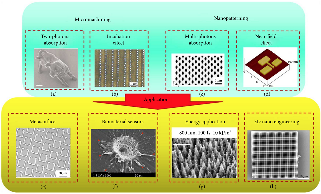 |
| Femtosecond laser precision engineering methods and the associated purposes: (a) bull sculpture produced by TPA, the dimensions bar is 2 µm, (b) microhole array fabricated on 150 µm Al movie by femtosecond laser direct scanning, (c) moist etching of nanopores fabricated by 3D femtosecond laser writing in YAG crystal, (d) unfavorable metallic oxide semiconductor patterns fabricated by femtosecond laser helping NSOM, (e) practical microstructures made by parallel femtosecond laser processing, (f) floor morphology of HP-PCL achieved by femtosecond laser microperforation, (g) SEM picture of laser microstructured Si floor fashioned in SF6 with femtosecond laser pulses, and (h) 3D practical photonic crystal fabricated utilizing 1030 nm femtosecond laser in a SZ2080 photoresist with out utilizing of picture initiator.
|
|
Moreover, the current progress about micro-lens arrays and interference lithography strategies for the sub-micron characteristic creation, particularly giant space periodic floor structuring, are additionally mentioned. For the femtosecond laser nano-fabrication, each the processing methods working in close to discipline and much discipline are summarized.
|
|
The outlook of femtosecond laser precision engineering can also be evaluated. Learn how to obtain small warmth affected zone is the primary key difficulty in prime quality laser precision engineering to push its decision from micro-scale to nano-scale.
|
|
Secondly, making certain a excessive sufficient processing pace to fulfill varied industrial wants can also be a key problem since one beam laser processing at excessive decision couldn’t meet this requirement.
|
|
The third problem is methods to perform the laser nano-structuring within the far discipline because the close to discipline impact requires tiny optics working very near pattern surfaces, which confines the close to discipline laser nano-fabrication to be solely appropriate for a number of super-smooth floor samples.
|

