(Nanowerk Information) Researchers fabricated a 14 cm tall Christmas tree with a thickness of 1 atom and confirmed how terahertz measurements can be utilized to make sure the standard of graphene.
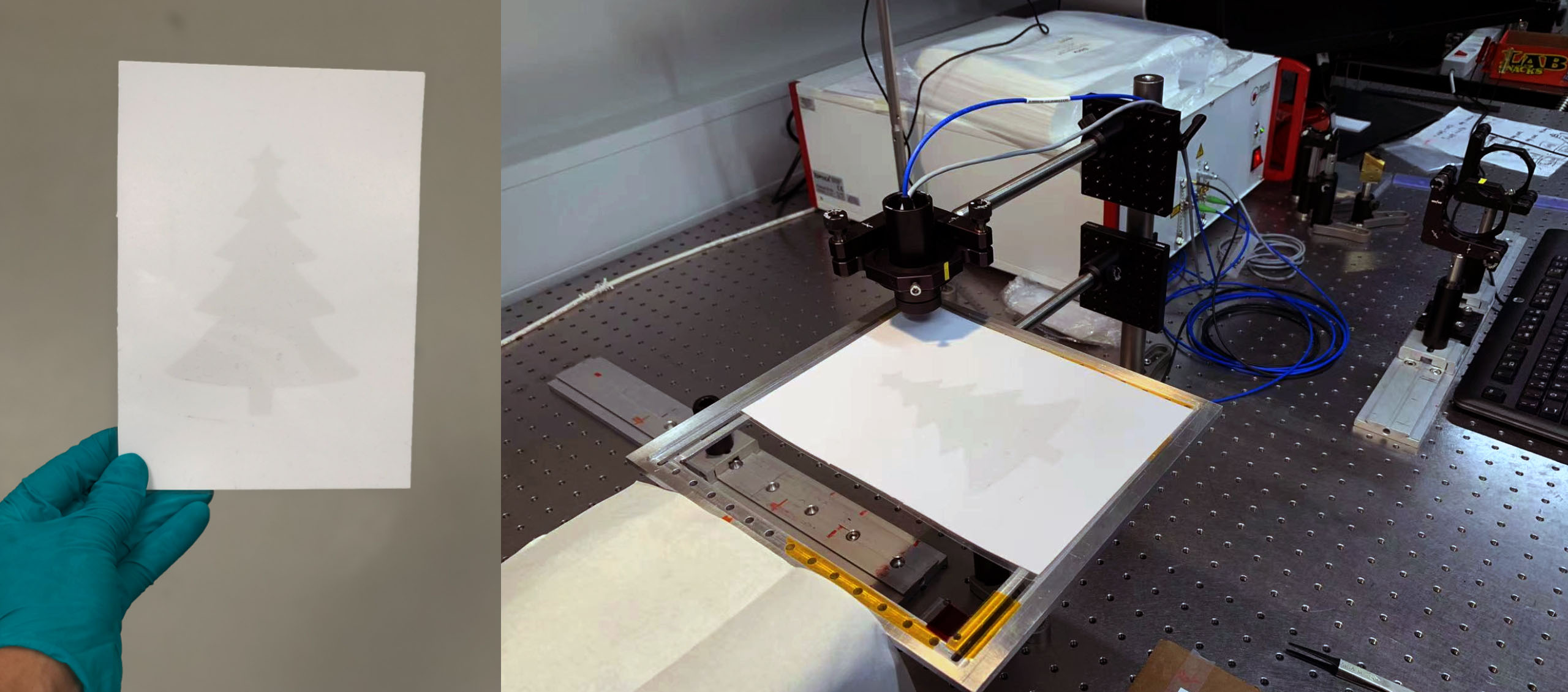
Graphene Christmas bushes. (Picture: Jie Ji)
The Christmas tree within the photos above is 14 centimetres tall. Since it’s product of graphene, it consists of carbon atoms in just one layer and is simply a 3rd of a nanometer thick. It’s reduce out of a 10-meter lengthy roll of graphene, transferred in a single piece utilizing a rebuilt laminating machine after which scanned with terahertz radiation.
The experiment exhibits that steady high quality management could be performed in the course of the manufacturing of graphene, which is predicted to play a major position in future high-speed electronics, i.e. medical devices and sensors.
Graphene is a so-called two-dimensional materials, i.e. it consists of atoms in a single cohesive layer that is just one atom skinny. It’s extra strong, stiffer and higher at conducting electrical energy and warmth than another materials we all know of. Due to this fact, graphene is an apparent candidate for digital circuits that take up much less area, weigh much less, are bendable and are extra environment friendly than the electronics we all know right now.
“Even in the event you might make a pencil drawing of a Christmas tree and carry it off the paper—which, figuratively, is what we’ve performed—it could be a lot thicker than one atom. A bacterium is, e.g. 3000 instances thicker than the graphene layer we used. That’s why I dare name this the world’s thinnest Christmas tree. And though the start line is carbon, identical to the graphite in a pencil, graphene is on the similar time much more conductive than copper. The “drawing” is made in a single excellent layer in a single piece, “ says Professor Peter Bøggild who lead the workforce behind the Christmas tree experiment.
Right here, the graphene layer is seen after switch from the copper roll and whereas being examined utilizing terahertz radiation. (Picture: Abhay Shivayogimath and Jie Ji)
“However behind the Christmas joke hides an necessary breakthrough. For the primary time, we managed to make an in-line high quality management of the graphene layer whereas we transferred it. Doing that is the important thing to gaining secure, reproducible and usable materials properties, which is the prerequisite for utilising graphene in, e.g. digital circuits.“
30,000 instances thinner than kitchen movie
Because the researchers have performed on this case, the graphene could be “grown” on copper movie. The graphene is deposited on a roll of copper foil at round 1000 °C. That course of is well-known and well-functioning. However quite a bit can go improper when the ultra-thin graphene movie is moved from the copper curler to the place it’s used.
Since graphene is 30,000 instances thinner than kitchen movie, it’s a demanding course of. Researcher Abhay Shivayogimath has been behind a number of new innovations in DTU’s switch course of, guaranteeing a secure switch of the graphene layers from the copper roll.
Furthermore, there was no know-how that would management {the electrical} high quality of graphene on the go – whereas transferring it. This yearPeter Bøggild and his colleague Professor Peter Uhd Jepsen from DTU Fotonik, one of many world’s main terahertz researchers, established a option to do it.
The colored photos are measurements of how the graphene layer absorbs terahertz radiation. The absorption is immediately associated to the electrical conductivity: the higher the conductive graphene, the higher it absorbs.
Terahertz rays are high-frequency radio waves that lie between infrared radiation and microwaves. Like X-rays, they can be utilized to scan human our bodies, as we all know it from airport safety. Terahertz rays may also take photos of {the electrical} resistance of the graphene layer. By connecting the terahertz scanner to the machine that transfers the graphene movie, it’s doable to picture {the electrical} properties of the movie in the course of the switch course of.
Official worldwide measurement commonplace
Suppose the implementation of graphene and different 2D supplies is to be accelerated. In that case, ongoing high quality assurance is a prerequisite, says Peter Bøggild. High quality management precedes belief, he says. The know-how can assure that graphene-based applied sciences are manufactured extra uniformly and predictably with fewer errors. This yr, the DTU researchers’ technique was authorized as the primary official worldwide measurement commonplace for graphene. Their technique was described earlier this yr within the article Terahertz imaging of graphene paves the way in which to industrialisation.
The potential is great. Graphene and different two-dimensional supplies can e.g. allow the manufacturing of high-speed electronics performing lightning-fast calculations with far much less energy consumption than the applied sciences we use right now. However earlier than graphene can grow to be extra widespread on an industrial scale and be utilized in electronics, we encounter in on a regular basis life three foremost issues have to be solved.
First, the value is just too excessive. Extra and sooner manufacturing is required to carry the value down. However with that, you face the second drawback: Once you improve the velocity and cannot on the similar time examine the standard, the chance of error additionally will increase dramatically. At excessive high-speed switch, all the things have to be set exactly.This brings us to the third drawback: How are you aware what’s exact?
It requires measurements. And ideally measurements in the course of the precise switch course of. The DTU workforce is satisfied that one of the best wager on that technique is high quality management utilizing terahertz radiation.
On this Youtube video prof. Bøggild explains the strategy intimately.
Peter Bøggild emphasises that these three issues haven’t been solved with the brand new technique alone: “We’ve got taken a really important step. We’ve got transformed a laminating machine right into a so-called roll-2-roll switch system. It gently lifts the graphene layer from the copper roll on which the graphene layer is grown and strikes it onto plastic foil with out it breaking, turning into wrinkled or soiled. Once we mix this with the terahertz system, we will instantly see if the method has gone nicely. That’s, whether or not we’ve unbroken graphene with low electrical resistance.”
The Terahertz technique was created in collaboration with researchers within the Danish innovation fund undertaking TRIM and the big EU analysis projectGraphene Flagship. DTU partakes in Graphene Flagship with the essential analysis centreCenter for Nanostructured Graphene.
