| Dec 23, 2021 |
|
(Nanowerk Information) Researchers on the RIKEN Middle for Emergent Matter Science (CEMS) and the RIKEN Cluster for Pioneering Analysis (CPR) in Japan have developed a method to enhance the flexibleness of ultra-thin electronics, resembling these utilized in bendable units or clothes.
|
|
Printed in Science Advances (“Direct gold bonding for versatile built-in electronics”), the examine particulars using water vapor plasma to immediately bond gold electrodes fastened onto separate ultra-thin polymer movies, without having adhesives or excessive temperatures.
|
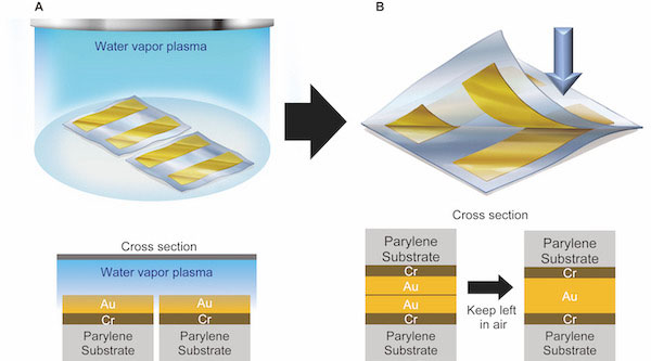 |
| (A) Evaporated gold surfaces on 2 µm thick parylene substrates have been uncovered to water vapor plasma. (B) Bonding of water vapor plasma treated-gold was achieved by overlapping the 2 substrates and storing them in ambient air for just a few seconds to a number of hours with none utilized strain or warmth. (Picture: RIKEN)
|
|
As digital units get smaller and smaller, and the need to have bendable, wearable, and on-skin electronics will increase, standard strategies of establishing these units have develop into impractical. One of many largest issues is easy methods to join and combine a number of units or items of a tool that every reside on separate ultra-thin polymer movies.
|
|
Standard strategies that use layers of adhesive to stay electrodes collectively scale back flexibility and require temperature and strain which might be damaging to super-thin electronics. Standard strategies of direct metal-to-metal bonding can be found, however require completely easy and clear surfaces that aren’t typical in a lot of these electronics.
|
|
A crew of researchers led by Takao Someya at RIKEN CEMS/CPR has developed a brand new methodology to safe these connections that doesn’t use adhesive, excessive temperature, or excessive strain, and doesn’t require completely easy or clear surfaces. The truth is, the method takes lower than a minute at room temperature, adopted by a few 12-hour wait.
|
|
The brand new approach, known as water-vapor plasma-assisted bonding, creates steady bonds between gold electrodes which might be printed into ultra-thin—2 thousandths of a millimeter—polymer sheets utilizing a thermal evaporator.
|
|
“That is the primary demonstration of ultra-thin, versatile gold electronics fabricated with none adhesive,” says Senior Analysis Scientist Kenjiro Fukuda of RIKEN CEMS/CPR. “Utilizing this new direct bond know-how, we have been in a position to fabricate an built-in system of versatile natural photo voltaic cells and natural LEDs.”
|
|
Experiments confirmed that water-vapor plasma-assisted bonding carried out higher that standard adhesive or direct bonding strategies. Particularly, the energy and consistency of the bonds have been larger than what commonplace surface-assisted direct bonding achieved. On the similar time, the fabric conformed higher to curved surfaces and was extra sturdy than what might be achieved utilizing an ordinary adhesive approach.
|
|
Based on Fukuda, the strategy itself is surprisingly easy, which could clarify why they found it by chance. After fixing the gold electrodes onto polymer sheets, a machine is used to reveal the electrode sides of the sheets to water-vapor plasma for 40 seconds. Then, the polymer sheets are pressed collectively in order that the electrodes overlap within the right location. After ready 12 hours in room temperature, they’re prepared to make use of.
|
|
One other benefit of this method is that after activation with water-vapor plasma, however earlier than being bonded collectively, the movies will be saved in vacuum packs for days. This is a crucial sensible facet when contemplating the potential for ordering and distributing pre-activated elements.
|
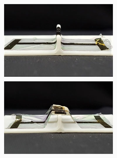 |
| Conformability check. Photographs from the conformability check on a curved floor (radius: 0.5 mm). Extremely-thin movies bonded utilizing (high) water-vapor plasma assisted bonding or (backside) commonplace adhesive. Conformability was significantly better for water-vapor plasma assisted bonding. (Picture: RIKEN)
|
|
As proof of idea, the crew built-in ultra-thin natural photovoltaic and LED-light modules that have been printed on separate movies and related by 5 extra polymer movies. The units withstood intensive testing, together with being wrapped round a stick and being crumpled and twisted to extremes. Moreover, the facility effectivity of the LEDs didn’t endure from the therapy. The approach was additionally in a position to be part of pre-packaged LED chips to a versatile floor.
|
|
“We anticipate this new methodology to develop into a versatile wiring and mounting know-how for next-generation wearable electronics that may be connected to garments and pores and skin,” says Fukuda. “The following step is to develop this know-how to be used with cheaper metals, resembling copper or aluminum.”
|

