

[ad_1]
Within the quest to maintain Moore’s Legislation going, you may think eager to shrink transistors till the smallest half was simply an atom thick. Sadly, that received’t work for silicon. Its semiconducting properties require a 3rd dimension. However there’s a class of supplies that act as semiconductors although they’re two-dimensional. And new outcomes from among the greatest chip firms and analysis establishments present that these 2D semiconductors may very well be a very good path ahead as soon as silicon’s limits are reached.
In work offered this week at
IEEE Worldwide Electron Gadgets Assembly, in San Francisco, researchers at Intel, Stanford, and TSMC offered separate options to one of the crucial vexing limitations to creating 2D transistors: sharp spikes of resistance on the locations the place the semiconductor meets steel contacts. In the meantime, engineers at imec confirmed each how they’re clearing a path to commercial-grade manufacturing processes and demonstrating simply how small future 2D transistors may be. And researchers in Beijing and Wuhan have constructed the 2D equivalents of essentially the most superior kinds of silicon units.
“Silicon has reached its restrict,” says Krishna Saraswat, a professor {of electrical} engineering at Stanford College. “Folks declare that Moore’s Legislation is over, however for my part that’s not the case. Moore’s Legislation can proceed by going within the third dimension.” For that, you want 2D semiconductors or one thing like them, says Saraswat, who collaborates with Stanford professors Eric Pop and H.-S. Philip Wong on 3D chips. Due to their potential to scale all the way down to small dimension and comparatively low processing temperatures, 2D semiconductors may very well be in-built a number of layers.
2D semiconductors belong to a category of supplies known as transition steel dichalcogenides. Amongst them, the most effective studied is molybdenum disulfide. Electrons ought to theoretically zip via tungsten disulfide, one other such 2D materials, extra rapidly than MoS2. However in experiments at Intel, MoS2 units had been superior.
Maybe the largest impediment 2D semiconductors face is making low-resistance connections to them. The issue is named “Fermi-level pinning”, however what it means is {that a} mismatch between the electron energies of the steel contact and the semiconductor creates a high-resistance barrier to the circulation of present. This Schottky barrier is created as a result of electrons close to the interface circulation into the lower-energy materials, leaving a charge-depleted space that resists present. The purpose now’s to make that area so insignificant that electrons can simply tunnel throughout it with out a lot effort.
Rival chipmakers TSMC and Intel individually hit on a special answer—antimony
Aravindh Kumar, a scholar of Saraswat’s, got here up with certainly one of a pair of options to the issue that had been reported at IEDM. In prior analysis, gold had been the contact of selection for forming transistors with MoS2. However depositing gold and different high-melting-point metals damages the MoS2, making the barrier downside worse. So Kumar experimented with indium and tin, which have melting factors within the low tons of of levels C.
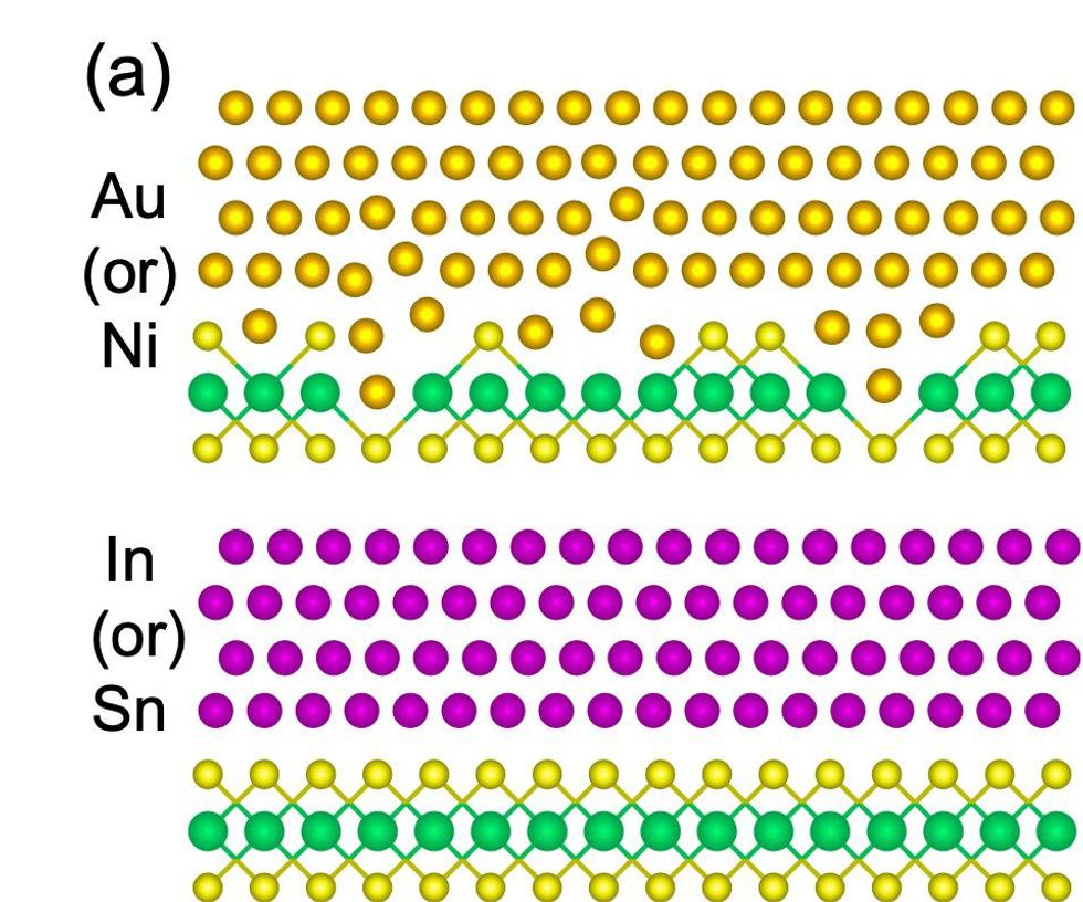
Depositing gold disrupts the 2D semiconductor. However indium and tin do no injury.Aravindh Kumar
However these values are so low that these metals would soften through the latter elements of the chip processing and packaging course of, which which exposes chips to temperatures reaching 300-500 levels C. Even worse, the metals had been oxidizing throughout processing. Whereas attempting to unravel the latter downside, Kumar fastened the previous. The reply was to alloy the low-melting level metals with gold. The indium or tin are deposited onto the MoS
2 first, defending the semiconductor, then they’re capped with gold to maintain away the oxygen. The method results in a tin-gold alloy with 270 ohm-micrometer resistance and indium-gold with 190 ohm-micrometer. And each alloys must be secure to a minimum of 450 levels C.
Rival chipmakers TSMC and Intel individually hit on a special answer—antimony. The concept is to cut back the vitality barrier between the semiconductor and the contact through the use of a semimetal because the contact materials, explains Han Wang, supervisor for low-dimensional analysis at TSMC Company Analysis. Semimetals, corresponding to antimony, are supplies that behave like they’re on the boundary between a steel and semiconductor and have zero band hole. The ensuing Schottky barrier may be very low, resulting in low resistance in each the TSMC and Intel units.
TSMC had beforehand labored with bismuth, one other semimetal. However its melting level was too low. Antimony’s higher thermal stability means it will likely be extra suitable with current chipmaking processes, result in longer-lasting units, and permit for extra flexibility within the latter a part of the chip making course of, says Wang, who labored with Stanford’s Wong within the latter’s position as TSMC chief scientist.
In addition to making higher units, researchers at imec are inquisitive about discovering paths to integrating 2D semiconductors on business 300-mm silicon wafers, says Inge Asselberghs, program supervisor for exploratory logic. Utilizing 300-mm wafers, imec to discover how small 2D units would possibly finally get. Utilizing tungsten disulfide because the semiconductor, the researchers shaped double gate transistors, the place the WS2 is sandwiched between high and backside electrodes that management the present flowing via. Using patterning methods, they managed to scale down the highest gate to beneath 5 nanometers. That exact machine didn’t carry out notably effectively, however the analysis pointed towards methods to enhance on it.
Individually, in analysis to be offered later this week, imec will present 300-mm suitable course of optimizations steps to enhance MoS2 transistor attribute by together with a gadolinium aluminate interlayer amongst different issues.

Imec made a tungsten disulfide transistor with a gate size lower than 5 nanometers.imec
Although double-gate units like imec’s are the norm for 2D analysis, engineers at Peking College, in Beijing, and at Wuhan Nationwide Excessive Magnetic Area Heart took issues one step additional. At this time’s silicon logic transistors, known as FinFETs, have a construction wherein present runs via a vertical fin of silicon and is managed by a gate that drapes over the fin on three sides. However, in an effort to proceed to scale down the dimensions of units whereas nonetheless driving enough present via them, main chipmakers are transferring to nanosheet units. In these, ribbons of semiconductor are stacked up; every is surrounded by the gate on all sides. Beijing researchers led by
Yanqing Wu, mimicked that construction utilizing two layers of MoS2. The machine turned out to be greater than the sum of its elements: In contrast with their single-layer units, the 2D nanosheets had higher than twice the transconductance, that means for a given voltage it drove greater than double the present.
Intel simulated an much more excessive model of the stacked 2D machine. Its researchers went with six layers of MoS
2 and solely a 5-nanometer gate size, as an alternative of the Beijing machine’s two layers and 100 nanometers, respectively. In contrast with a simulated silicon machine of the identical vertical top and with a 15-nanometer gate size, the 2D machine packed in two extra nanosheets and carried out higher. And all that was although electrons journey extra slowly via MoS2 than via silicon and that the contact resistances are a lot greater.
Wu and colleagues then took one other step towards mimicking the near-future plans of silicon machine makers. CMOS chips, by definition, are made up of pairs of N-MOS and P-MOS units. As a solution to cram much more units into the identical space of silicon, chipmakers wish to stack the 2 sorts on high of one another as an alternative of arranging them side-by-side. Intel demonstrated such a silicon machine, known as a
complementary FET (CFET), finally 12 months’s IEDM. Wu’s staff tried the identical by changing one of many MoS2 layers of their stacked machine with tungsten diselenide. Then, by modifying the connections between the supply and drain, the 2D CFET grew to become an inverter circuit, with primarily the identical footprint as a single transistor.
There’s clearly numerous work to do earlier than 2D semiconductors achieve a spot in mass manufacturing, however with the progress made on contact resistance and the potential proven by the brand new experiments, researchers are hopeful.
This publish was corrected on 14 December to make clear imec’s analysis contributions.
From Your Web site Articles
Associated Articles Across the Internet
[ad_2]